If you followed the last week of Vectorblade beta tests in the forum, you might have read about Peers “special” Vectrex. It was special in the way, that it crashed playing Vectorblade (- or more precisely during startup).
We pinned that behaviour down to the VIA chip. I sent Peer a known working VIA, he inserted it – and it more or less works now. Nonetheless, we both were interested, what was happening, and is it indeed a hardware bug, or is it a special feature of some kind?
Anyway, Peer sent me the “faulty” VIA – and I tried to examine more closely to the best of my ability – what follows is a short summary of what I did today.
1) I put the Peers VIA into one of my Vectrex, and tried different things.
a) Vectorblade -> CRASH (192k Cartridge)
b) Robot Arena -> CRASH (64k VecFever)
c) Thomas’ emulators -> WORK (64k VecFever)
d) VectorPatrol -> CRASH (64k Cartridge)
e) VectorPilot -> WORK (64k Cartridge)
WOW! This does not make much sense!
2) New startpoint, since I know Vectorblade best at the moment, Vectorblade will be my main testobject.
3) We / I had the idea, that different VIA exists and that they might internally be slightly different. The layouts given in the manuals seemed to say, that the Port B input/output circuits might be slightly different, especially in relation to “pull up” resistors used.
I tried different (and gradually changing) setups with adding own pull up resistors, but to no avail. Either I pulled to much up – and the zero point could not be reached any longer, or the behaviour was exactly the same – even using very small different resistor steps.
4) After that I tried to locate EXACTLY the place, where my own program Vectorblade crashed – which wasn’t as easy as it sounds, since depending on the variations used, it crashed at very different locations (Heisenbug).
Finaly I was able to find one spot, that sort of made sense, the bankswitch from bank 3 to bank 2.
(which in the following I will name switch from bank 1 to 0, because it is more common to only think in two banks).
Little interlude: “classic” Bankswitching
Since John invented it some time around 1998 the classic Vectrex bankswitching uses the “external line”, which is the only general purpose line, that goes to the cartridge port (cartridge line 35).
That external line is directly connected to the VIA 6522 chip, more precisely to Port B of via, even more precisely to bit 6 of VIA port B. Therefor in the following we will call that thing PB6.
PB6 (meaning the external line) is used as an additional addressline for the cartridge port. Usually vectrex carts have a maximum of 32k addressable ROM space, using bankswitching you can double that. The PB6 (external line) than is configured as the highest address line and switches thus between the lower and upper 32k of a 64k address space.
The default state (when vectrex powers up) is “1” so if you use a bankswitch cartridge the “powerup” memory space is from the cartridge view $8000 – $ffff which is “mapped” to the vectrex ROM space $0000 – $7fff.
PB6 is controlled by the VIA chip, which can be controlled by the programmer. But controlling PB6 directly has its quirks, since VIA port B is used “always”. If you print a vector, if you print a string, if you output sound or read joystick data – ALWAYS for these things you must in someway write a value to VIA port B. If you do bankswitching by “changing” bit 6 of VIA port B, you must write ALL these functions new, one version for bank 0 and one version for bank 1.
Now, John Dondzila the “inventor” of the bankswitching did some clever thinking and came up with the following:
The complete port B of VIA is nothing more than a general purpose input/output byte (for vectrex it is not completely general purpose though).
All bits can be configured individually to be input bits or output bits.
Now – what John figured out was, that
a) when PB6 is configured as INPUT – than from the cartridge port side the state of the line is always HIGH, meaning when PB6 is in input mode ALWAYS Bank 1 is active
b) when PB6 is configured as OUTPUT – than from the cartridge port side the state of the line is always the value, that you last put into PB6
c) every BIOS function that uses port B puts a ZERO into PB6
Keeping above in mind – than a simple switch between HIGH and LOW PB6 can be done using not the PB6 itself, but configuring PB6 as input (when it should be HIGH) and configuring PB6 as output (when it should be low).
The configuration whether it should be input or output is done with the DDRB (DataDirectionPortB) register of VIA, which is very seldom used (actually it is not used by any original cartridge or the BIOS – except in the one time VIA initialization at the beginning).
Now… I more or less “located” a spot where a crash occurs. The quotes indicate that it was not easy, and actually the crash I actually examined is in the “observer” routine of my debugging. Yes here it is totally true, the observer changes the behaviour of the observed – but as it turned out – this was “ok”.
My “debugging” on the live Vectrex consisted of printing a number on the vectrex screen. If I could still see the number when running the program THAT particular spot was still ok, if I didn’t see the next number – than the bug/crash occured befor. Very straight forward.
What it came down to was this:
I printed a number BEFOR bankswitching and AFTER bankswitching – and I didn’t see the second number – which led me to believe that the bankswitching was wrong – which it wasn’t. The crash as it turned out (after many gray hairs) happened while I was printing the number! Actually the crash more or less happened in the BIOS routines!
Anyway, what I did next was to print the debug statements WITHIN the bankswitching routine.
Interlude: Bankswitching routines
Bankswitching routines are a bit “special”, because from one cycle to the next the whole address space changes. Therefor you put bankswitching routines in “neutral zones”.
Neutral zones here being address spaces that are not changed by bankswitching. There are two ways to achieve that:
a) put the routines in RAM, the RAM is located at $c800 onward, and is not influenced by bankswitching in any way
b) put EXACTLY the same routines at EXACTLY the same location in both banks. That way, when a bankswitch occurs the current instruction can continue (although in a different bank) at exactly the same spot.
So I put the debug printing within the “neutral zone”, than the printing was ok and the crash happened later. (One printing befor switching, one printing after switching):
bla bla bla…
After many more tryouts and gray hair – I took out my oscilloscope, and prepared a special vectorblade cartridge with measuring points. Than I was able to measure the output to PB6.
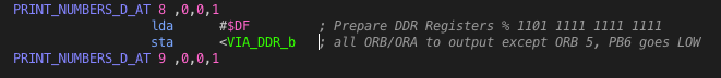
Here an image while still in bank 1:
Horizontally is more or less one Vectrex round (1/50s).
Vertically one square are two Volts, it is not centered very well in that picture.
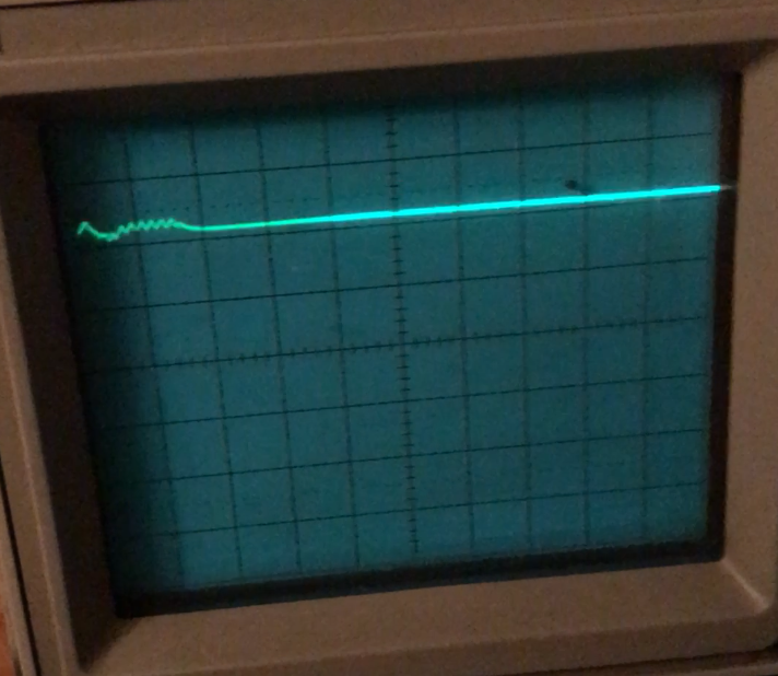
This is what it looks like on “normal” Vectrex in bank 0:
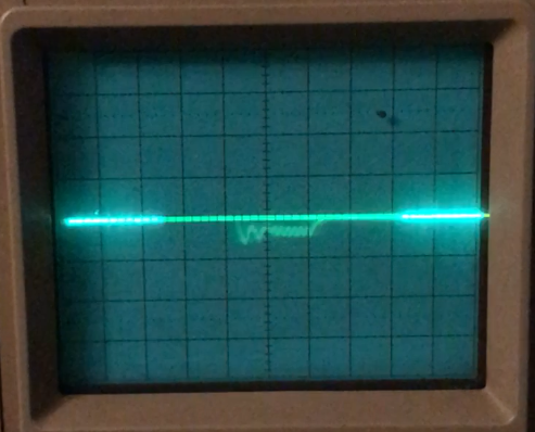
And this is what it looks like on our “problem” vectrex:
The dots in the beginning are “crash points”. Here PB6 switches to high without me telling it to do so.
Weird!
After some thinking I came to the conclusion, that the “disturbances” in the first image and the “dots” in the last image are:
a) “connected”
b) in the beginning of the Vectrex round I do the printing of the string. So the disturbances and the dots are done during my String printing!
Now I ripped my String printing apart. Found the first “dot” in Moveto_d, and ripped the Moveto_d appart…
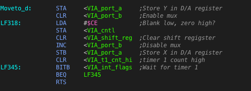
This is the “essence” of the Moveto_d. I tore that appart (meaning I tried each line on its own and tested whether it had any influence on PB6).
As it turned out the culprit is:
INC <VIA_port_b
This instruction – more precisely the first part of it – behaves differently with the VIA of Peer!
Above statement can be written as:
LDA <VIA_port_b
INCA
STA <VIA_port_b
Which certainly is “longer” and uses a register which in its short version (INC) it doesn’t – but it shows you exactly what INC does, it READS from VIA. And Peers VIA reads for PB6 a ONE – all other VIAs I have access to read ZERO!
And if it reads a one for PB6 it will STORE a one for PB6 in the statement following! And if it stores a one while PB6 is in output mode the cartridge receives a high state for the address line and a bankswitch occurs!
NORMAL VIA in output mode:
put 0 in PB6 -> the cartridge will read 0, vectrex will read 0
put 1 in PB6 -> the cartridge will read 1, vectrex will read 1
Peers VIA in output mode:
put 0 in PB6 -> the cartridge will read 0, vectrex will read 1
put 1 in PB6 -> the cartridge will read 1, vectrex will read 1
It must be said, that I could not find any documentation how VIA really “should” behave. I guess the behaviour is actually undefined.
(After all, PB6 is configured to OUTPUT (Vectrex should write to PB6), but instead the Vectrex reads PB6).
The “crash” – involuntary bankswitching – can occur anywhere, where VIA_PortB is not actually written to directly, but indirectly by INC or DEC statements! And the crash will only manifest when “neutral zones” are exited (the whole BIOS is a neutral zone for that matter).
Actually I now believe the VIA chip of Peer is not “buggy” or faulty per se.
I believe it was build slightly different than other VIA. For original Vectrex “times” the difference didn’t matter, since bankswitching came much later, it was invented and used by homebrewers.
Luckily there seem to be very few of these VIA in Vectrex all over the world, otherwise we would have heard screams for non working cartridges befor.
The whole situation can very easily be remedied by exchanging the VIA. A new VIA costs less than 2$, and all to me known Vectrex have the VIA in sockets. So it is just a matter of having a screwdriver and willingness to open the vectrex (beware the possible high voltage!!!).
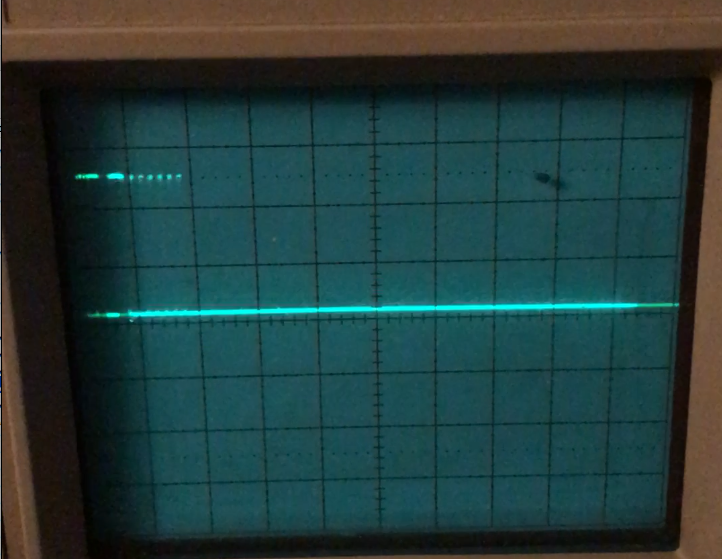
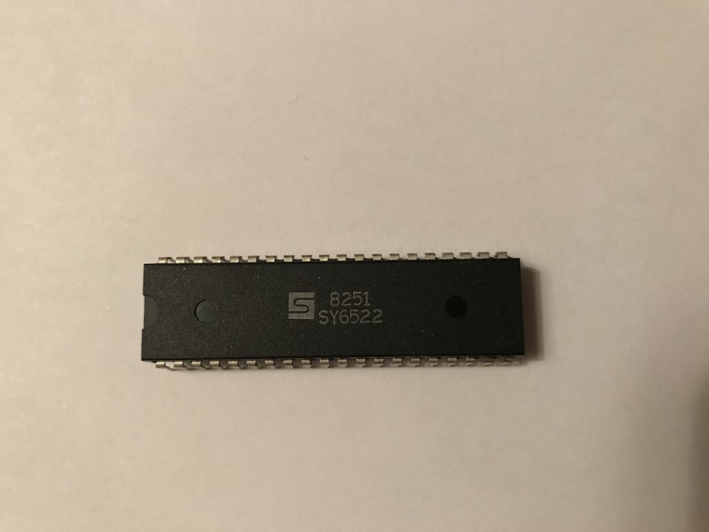
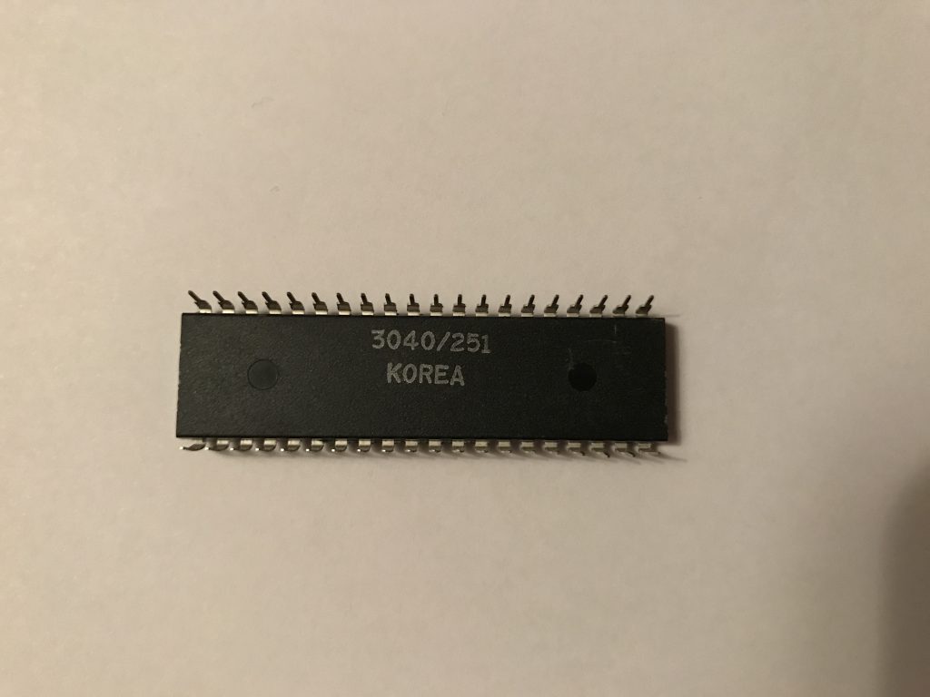
Following two images of the VIA I was talking about the whole time:
I have also written a test program, whether a VIA is prone to the “weird” behaviour:
- http://vectrex.malban.de/WeirdTest2.bin (updated, only 148 bytes now!)
(If your VIA is a “normal” one it say “normal VIA” if your Vectrex is a weird one – it says a “weird VIA” 🙂 )
I have not yet estimated, whether I will change Vectorblade to be compatible. That would actually include changing many, many functions and also filtering out all BIOS functions that use a “dec/inc” of VIA for PB6 bank(s) 0.
I will think about it – but I don’t know if I even have the space left – to use own functions for all circumstances in “bank(s) 0”.
This analysis (as usual) is top-notch! Thanks! I learned so many things about VIAs during our experiments, and now I also learned about all the very interesting internal details of bank switching in general and in VectorBlade. Great explanations!
Interesting analysis. So we all have to run the test bin on our VIAs and report back the results and IC info. It’ll be like hunting for Willy Wonka’s 5 golden tickets, but hoping to not find one. How exciting!
Hehe – in the moment I saw your comment popping up – I was watching your FORTH 3 video…
Yes – please go VIA hunting.
It would be VERY interesting indeed, if that VIA is actually broken – or all VIAs in that series behave like that!
Interesting.
I don’t know if some internal schematics of the VIA is published somewhere, but on any modern chip/µC this is the symptom of a fried input circuitry.
What you write always update the state of the output circuitry
What you read is always the state of the input circuitry
And the R/W mode connect and disconnect vcc/gnd of the output circuitry and pull-up of the input circuitry if tri-state is supported.
Did you find any other odd VIAs yet?
Nope 🙂
One of my Vectrex “turned” faulty (was ok before). So by now I think this might be a problem with indeed FAULTS within the VIA.
Anyway still – “normal” Vectrex programs will not be effected, as of now only bankswitching programs, which in wrong places inc/dec Via port B are effected.
I have compiled vectorblade from the final source on github, and it crashes on my late 3GE MB non Buzz Vectrex when running from a Vecmulti. Everything else works, including VectorPatrol, VectorPilot and Vectrexians (from their own PCB). Vectorblade_Gold_04 also crashes, so I guess its not a case of my compiled version. Title Screen comes up, then screen collapses and goes dark.
Even the test program “Weird Test” crashes with a blank screen, while it manages to come up with “normal VIA” on an Vectrex Emulator.
Changed the VIA to another one – same behaviour. Is it the Vecmulti?
Vectorblade does NOT run on a VecMulti card. Bankswitching for 4 banks is not supported by vecmulti. The maximum allowed vectrex bin size is 64kB for VecMulti, Vectorblade is either 192kB or 256kB (depending how you organize the banks).
This has nothing todo with the VIA.
Oh, thanks for the comment. I was under the impression from this thread: http://vide.malban.de/forums/topic/peer-testing-notes-findings-suggestion-etc/page/3 that it would work. Obviousky misintrepreted the lines “Richard Hutchinson VecMulti (n binaries with menu) works perfectly fine” thinking it would mean Vectorblade from Vecmulti. Not Vecmulti alone.
I will order some PCBs then. Thanks again!
The beta 5 should work.
And in general the VecMulti with the VIA.
The “final” (or near final) Vectorblades don’t.
I can report: after building a PCB for Vectorblade it runs super fine on my Vectrex. Such a fantastic game, I can’t believe it.
This is vector heaven. It must be.