Vectorblade.
Is driving me still nuts.
I more or less decided to do the “bosses” next. Last time I showed you parts of the new insect boss. Meanwhile I have progressed to the next boss – the Sinistar themed levels now also have an own boss.
I uploaded a short video of the encounter to youtube, see:
Also – again I am afraid I will sooner or later get into memory trouble. While it is part of the fun of programming a retro console – to optimize stuff and squeeze bits and bytes – I also have a “vision” how I would like Vectorblade to be. And still I am afraid 64kB will not suffice.
Two possible solutions:
– change my vision
or
– get more memory.
Several Facebook discussions, Proboard “talks” and emails later…
I STILL will try to get Vectorblade done in 64kB but meanwhile I will also seek for possible other solutions. One possible solution I followed the last couple of days I will describe in this post.
During above mentioned “talks” following possibilty emerged, which gives me 1/3 more memory, namely 96kB. Graham asked innocently in one of these “talks” why can’t we use the memory between $8000 and $bfff?
The simple answer is – we can! Just nobody did! (apart from blending in some RAM or using certain addresses as “HotSpots”)

The mentioned address space $8000 – $bfff features an additional 16kB of memory – thus if your cartridge is slightly redesigned – you can use 48kB of “straight” memory, from $0000 – $bfff. If you use the same address space with the “classic” PB6 bankswitch technique – you get twice as much -> 2*48kB -> 96kB.
This is what I am testing out just now.
The “classic” cartridge
uses only address lines A0-A14 (yellow) and can address the range from
$0000 – $7fff.
“Every” cartridge can use this memory (old original cartridges might have saved some copper and not connected the address lines though). Here you use eproms or memory chips with up to 32kB (or less depending on your memory allowence).
The ~CE is connected to A15 (green). Chip Enable is zero active. Meaning, when “0”, than the chip is enabled (haha). Every RAM/ROM/Eprom etc has a CE flag. This flag tells the chip whether it should answer “questions” asked to the BUS.
IF on the BUS an address is received which falls in the range of the chips address “possibilities” AND the Chip Enable flag is set to enabled, THAN the chip “answers” to the request (putting values on the data lines of the BUS).
For the default this is easy – everything in the first 32kB will be answered from the cartridge port, thus ~CE is very quickly realized with address line A15.
The classic PB6 cartridge
uses only address lines A0-A14 and can address the range from $0000 – $7fff. Furthermore the PB6 line (blue) is connected to the A15 line of the memory chip. So from the memory chips point of view it is just that – the highest possible address line, which denotes either +32768 or +0 to the actual address range.
If pb6 is set, than each address read from the memory chip has 32768 added – which effectively gives us an address range from $0000-$ffff (from the cartridge point of view).
Here you use eproms or memory chips with a up to 64kB.
~CE same as above.
The 48kB / PB6 cartridge (new design)
uses address lines A0-A15 (A15 = green) and can address the range from $0000 – $ffff (attention! – we do not want to use $c000-$ffff!).
Furthermore the PB6 line (blue) is connected to the A16 line of the memory chip. So from the memory chips point of view it is (again) just that – the highest possible address line, which denotes either +64768 or +0 to the actual address range (same as above but one bit higher).
If pb6 is set, than each address read from the memory chip has 64768 added – which effectively gives us an address range from $00000-$1ffff (from the cartridge point of view).
Here you use eproms or memory chips with a up to 128kB.
~CE now must be handled differently. If ~CE were connected as above we would only be able to access memory for the “lowest” 32kB of each of our new 64kB banks.
I will not explain too deeply here what is happening – but using boolean logic we come up with:
This means the “new” ~CE flag must be calculated using the address lines A14 and A15. Basically this means ~CE = zero when A14 OR 15 is zero. Or differently said ~CE is 1 when both A14 and A15 are 1. In numbers this means if the address given via the address lines A0-A15 < $bfff than the ChipEnable register is set to enabled, otherwise not.
Eagle
Now – that I knew the above “basics”, I quested on how to get a cartridge PCB done. I heard of “eagle” – one of many layout programs. For whatever reasons that was my first choice and for really small pcb’s it is freely usable.
I downloaded it and tried first tentive steps – and it drove me nuts! I asked around – but actually got not really much help – so I quested further on my own untill I got a little “feeling” for the software (and a soar mouth from swearing).
Than I found Franks Vectrex PCB design (link: https://hackaday.io/project/28295-vectrex-cartridge) – which I could use as a starting point.
(size of the PCB, placement of the holes, cartridge connector etc…)
Thank you Frank, for making that freely available!
This is what I produced after about 10 hours (I guess) after first downloading eagle: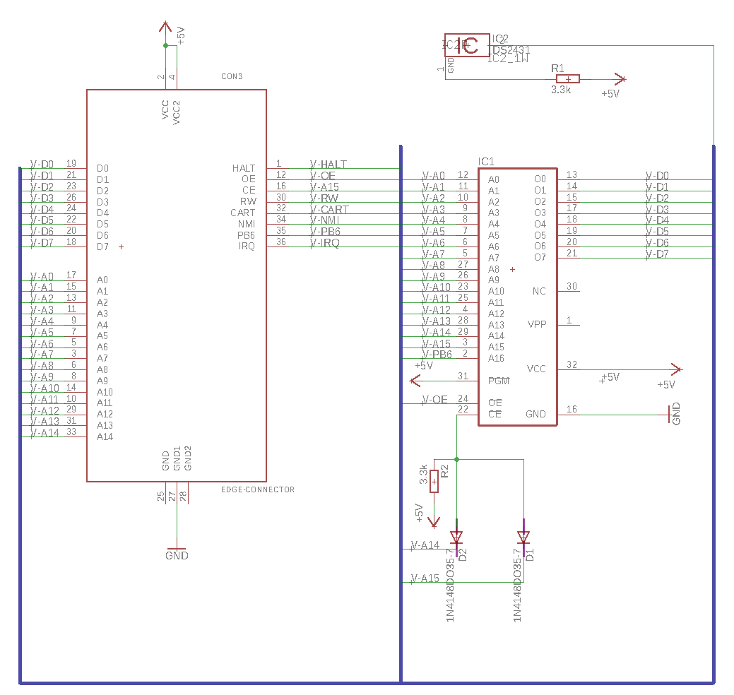
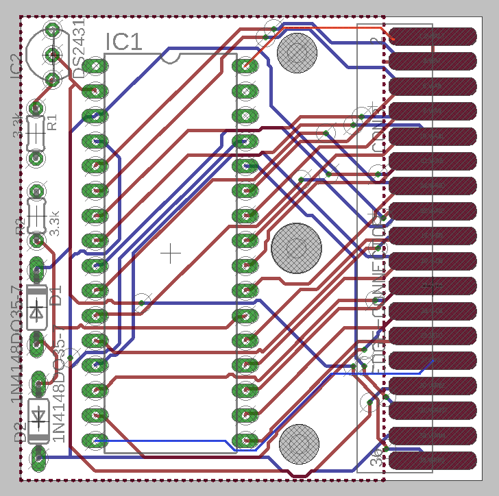
Ok, ok not beautifull – but I hope it will work out fine! This is a prototype!
Speaking of prototyping…
I always said I am a software guy – not a hardware guy.
At least partially I want to change that. I updated my workspace this week to:
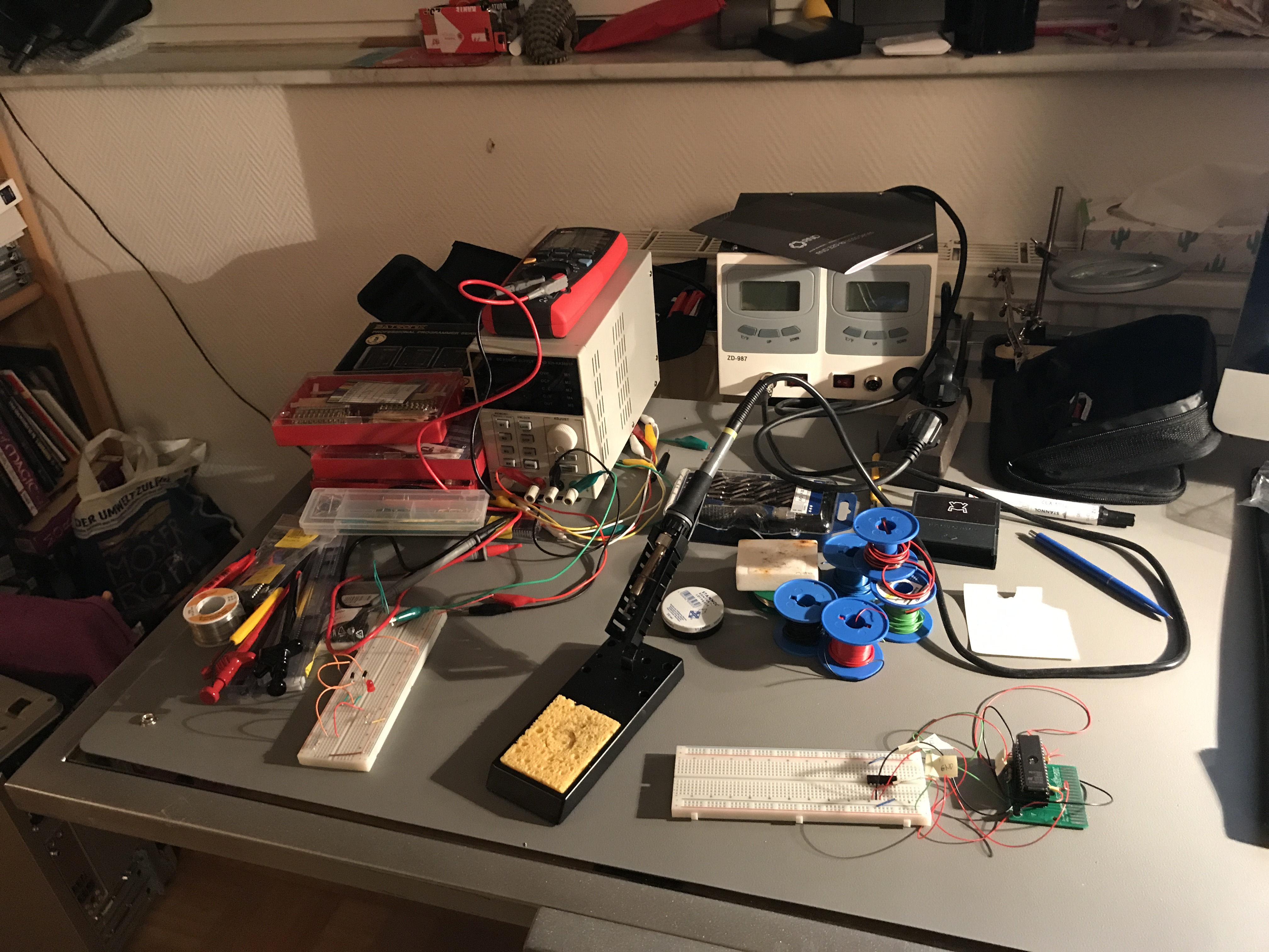
Because – above “theory” is all well – but before ordering that fancy design – I would like to test it first.
Prototyping step 1
Changing Vide to support 48kB bankswitching – done (in about 1/2 hour)
Prototyping step 2
Writing a program to test 48kB bankswitching (resulting in a 128kB bin file) – done (in about 10 minutes)
Ordering and sorting electronic
Which I did not already have lying around – this took actually a couple of days.
AND gate / or DL?
Above ~CE logic is an AND. How will I realize an AND on the PCB? Never done electronic – Ordering an AND gate and do breadboarding using an LED.
Didn’t get it to work Hmpf.
Using Diode Logic to implement an AND -> and using LED to test:
(yes – I know babysteps)

Uff – working!
“Upgrading” clockwork PCB
To test the above circuit I upgraded a known PCB.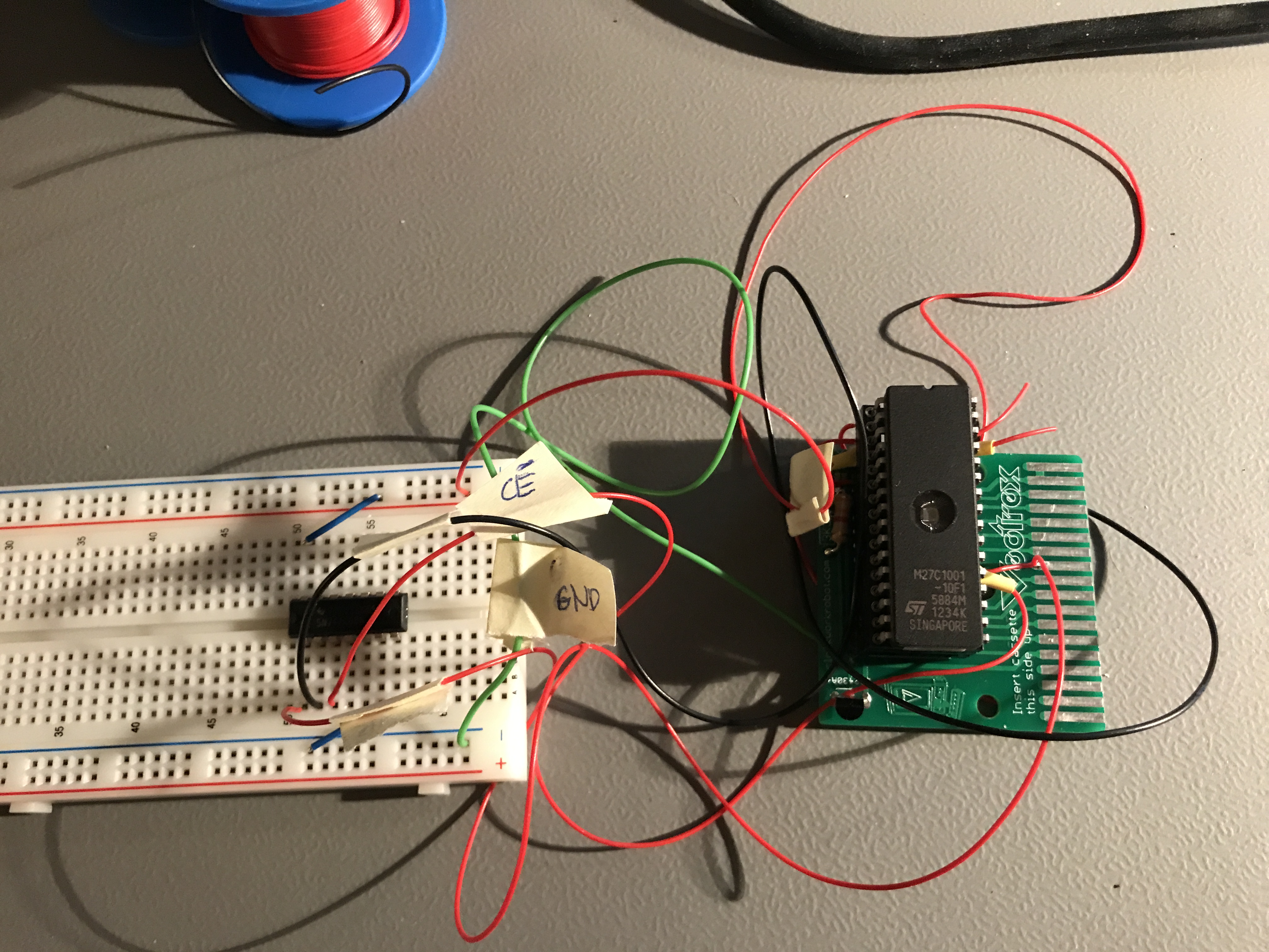
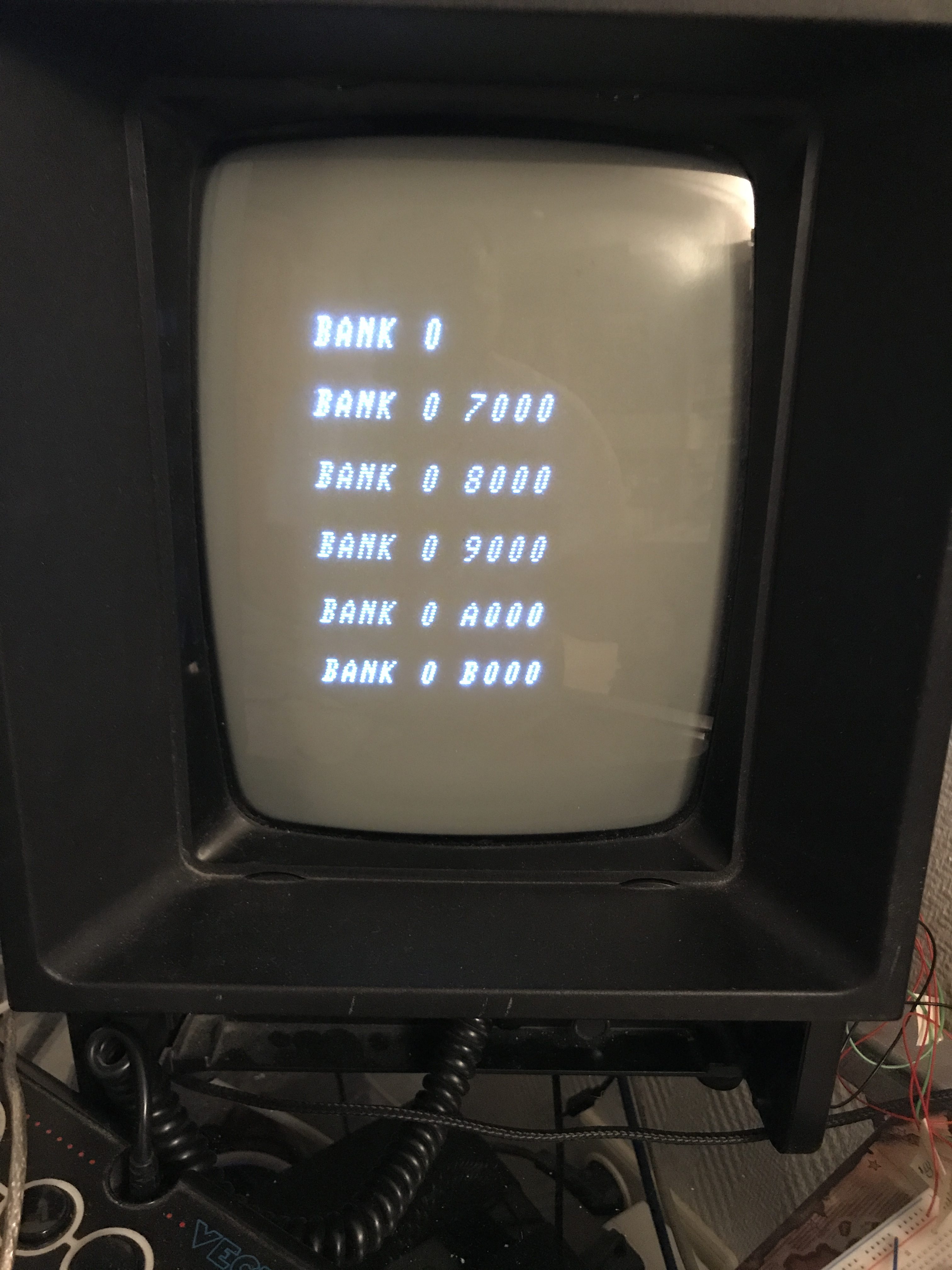
Here I use the AND gate chip. First try on a Vectrex – WORKING. I’ll be damed! STRIKE!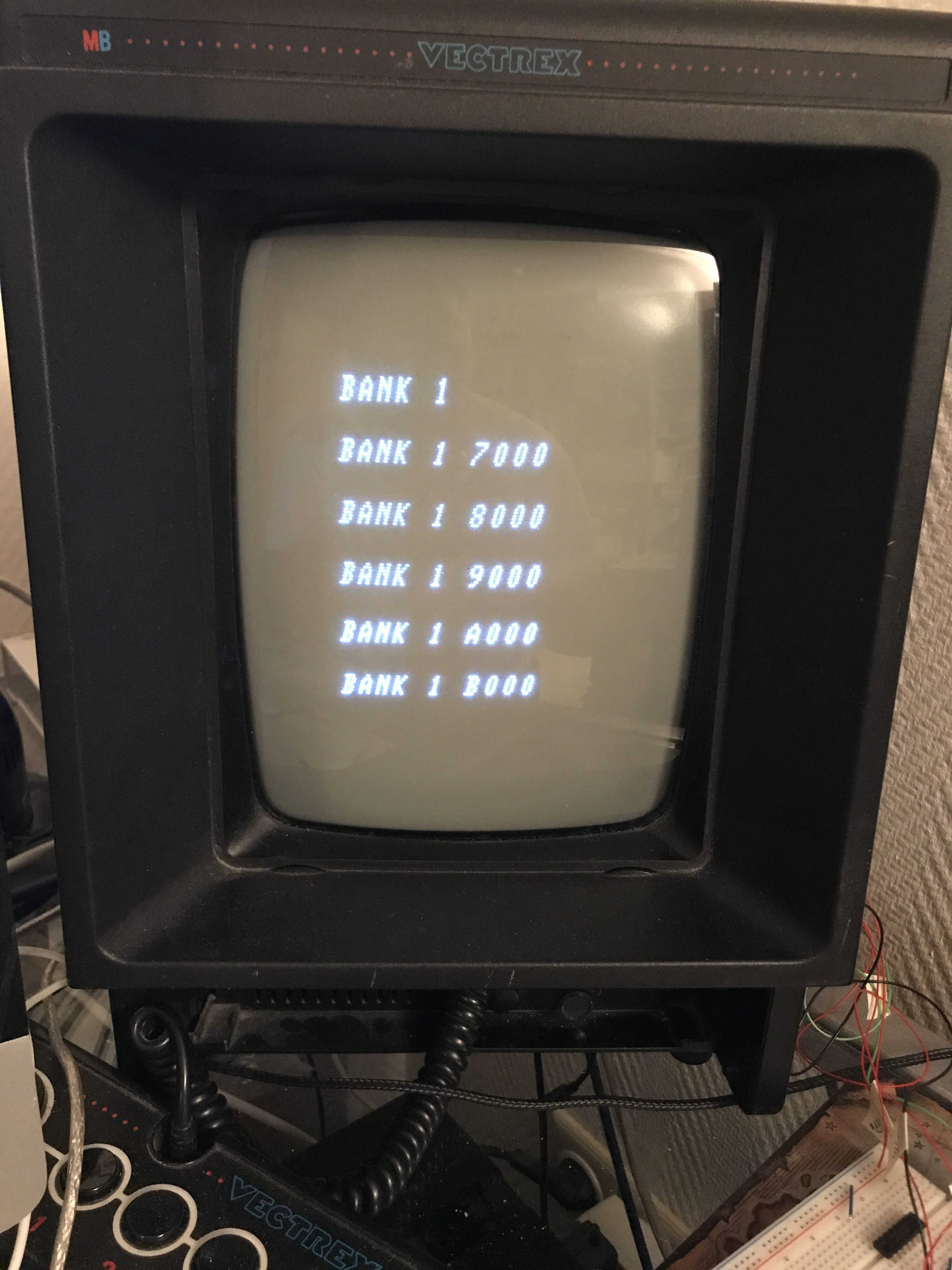
Now – there is not much space on the PCB, I’d rather prefer Diode Logic:
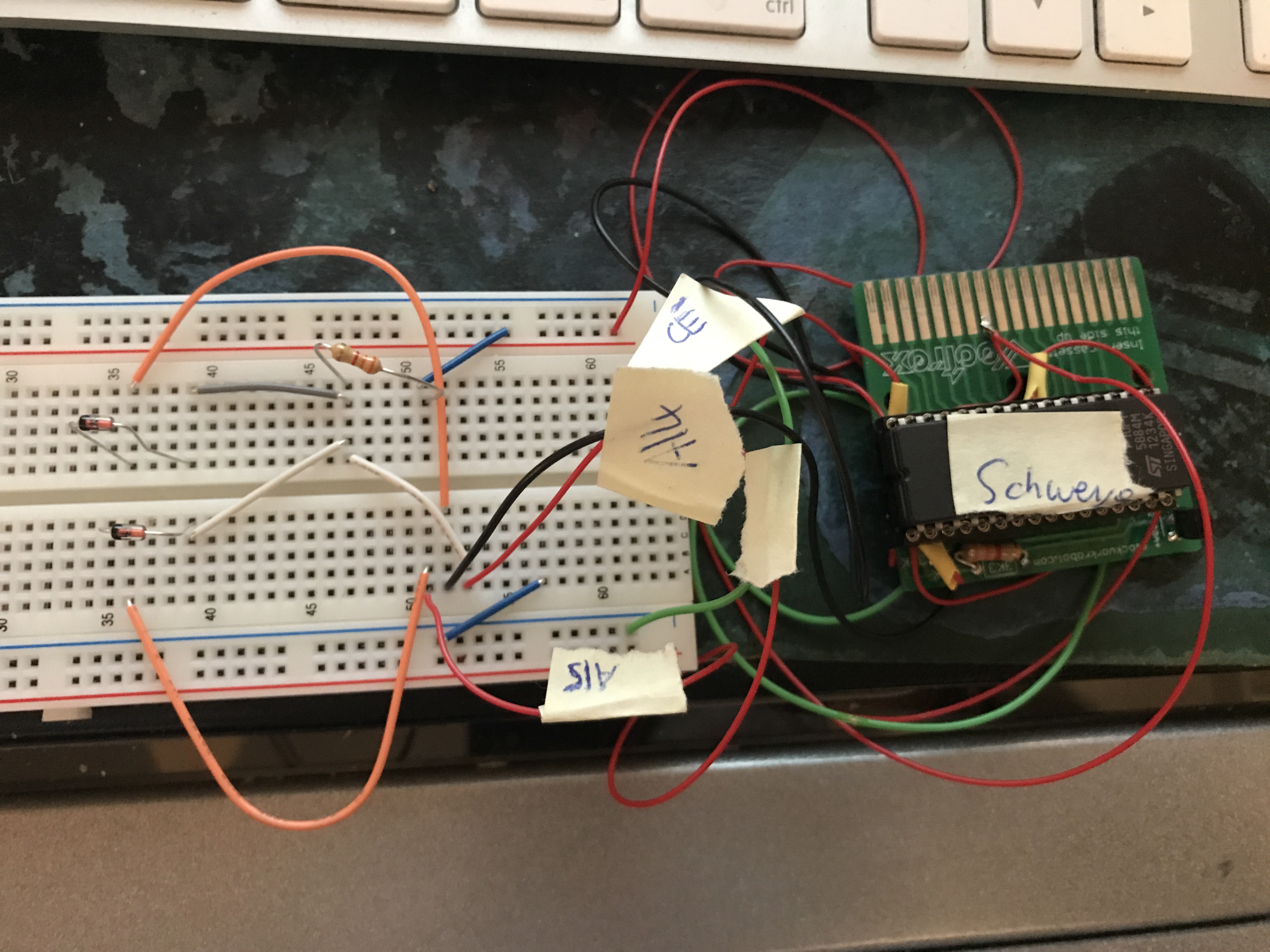
Ok, this did not work out of the box. I calculated the resistor wrong (well didn’t calculate at all). Using trial and error due to me not understanding electronics all to well – I now use a 3,3kOhm resistor, and it WORKS!!!
Updating the Eagle layout – and searching the web, resulted in:
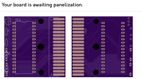
Me ordering a prototype of my first PCB. PROTOTYPE! Yeah, I know I could draw a small Karl Quappe on it… but guys – really – prototype!
Also:
Thomas is in Germany for two days – and with a wink of his hands, he updated VecFever to support 48kB Bankswitching – although it does not work with the RAM-drive option. But Hip hip hurray anyway!
See ye!
Malban